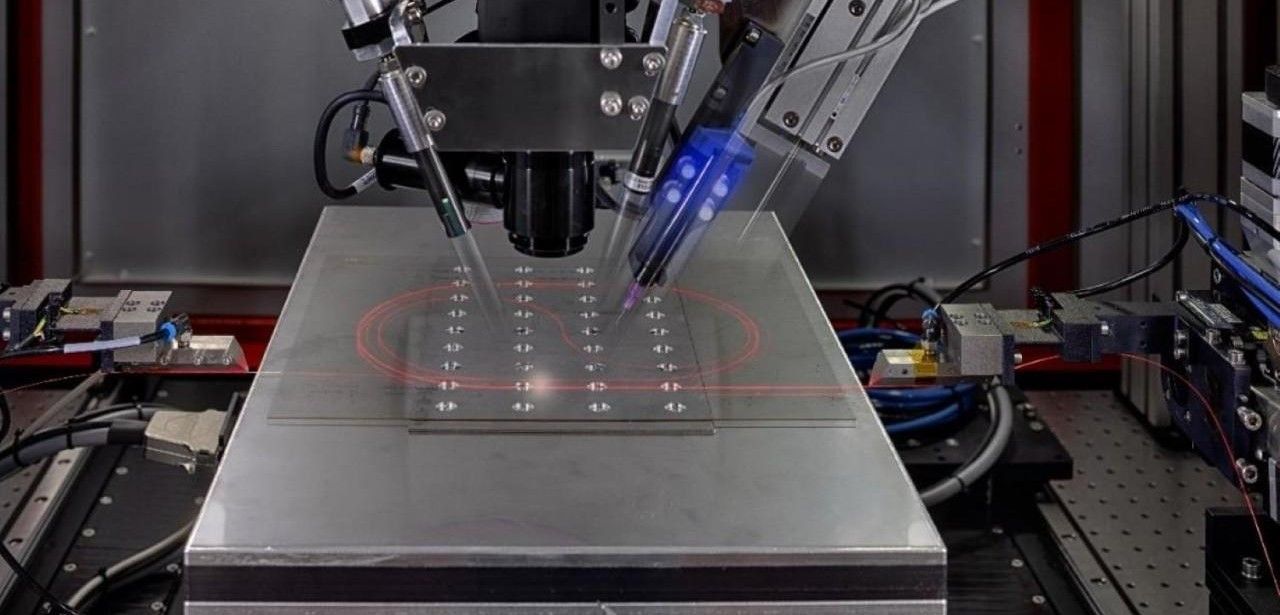
The use of glass as a substrate in electronic manufacturing offers numerous advantages. Not only does it enable the transmission of optical signals through the substrate material, but it also contributes to significantly higher data transfer rates in automotive, telecommunications, and AI applications. Researchers at Fraunhofer IZM have successfully developed a system within the research project “Integrated Electro-Photonic Panel Systems” (EPho) that automates the characterization of propagation losses in integrated optical waveguides.
Glass as a Substrate Material: Enhancing Data Transmission
In an increasingly digitized world with rapidly growing data volumes, new solutions are needed to efficiently process and transmit data. The miniaturization of transistors and their interconnection is reaching its limits in data centers and high-performance computers. To increase the number of transistors per package and achieve even higher power densities, chiplets are used. However, effectively connecting these chiplets requires a substrate with high requirements. Glass, as a substrate material, fulfills these requirements and enables the integration of optical waveguides. This allows for electro-optical circuit boards to transmit both electrical and optical signals, significantly increasing data transmission.
The Fraunhofer IZM has developed a process for producing low-loss single- and multi-mode waveguides in large-format thin glasses using ion exchange techniques. Inspecting these glass panels presents a challenge due to the large number of waveguides. To address this, an automated system has been developed to characterize the propagation losses of integrated waveguides. This includes waveguides written using femtosecond lasers or located in other substrate materials. The measurement process is consistent: a sample is inserted, the layout is uploaded, the waveguides are selected, and the measurement is initiated. The system automatically detects the edges of the substrate, any existing markings, and the precise position of the measurement fiber. Subsequently, the insertion losses of all selected waveguides are measured automatically.
The developed system offers extensive process control for the manufacturing of optical waveguides. It allows for the investigation of thousands of parameter sets in order to determine new process parameters during the development of waveguide manufacturing processes. Particularly in technologies with numerous variable process sizes, such as laser writing of waveguides, the system enables significant advancements to be made in a short period of time.
The research project EPho has been successfully completed and was funded by the Federal Ministry of Education and Research (BMBF) with a grant of 1.33 million euros. In addition to Fraunhofer IZM, other project partners such as ILFA GmbH, Schröder Spezialglas GmbH, and FiconTEC Service GmbH were involved.
The use of glass as a substrate in electronics manufacturing offers numerous advantages, including increased data transmission and efficient process control. By integrating optical waveguides, electro-optical printed circuit boards can transmit both electrical and optical signals, significantly enhancing data transfer. The developed system by Fraunhofer IZM allows for extensive process control and the determination of new process parameters in the production of optical waveguides. The EPho research project, funded by the BMBF, has been successfully completed.
The provided translation is a human-generated version and may not accurately convey the precise tone or style of the original article. It is important to consider that nuances and subtleties of the original text may be lost in translation, potentially affecting the overall message.


